
ECE4803B: Theory and Design of Music Synthesizers
Spring 2006
Homework #3
Due: Wednesday, Feb 22 at the start of class
The
Buchla Music Easel,
which consists of a Buchla 208 Programmable Sound Source and a
Buchla 218 Model Keyboard together in a single case, is one of the rarest
and most coveted of the Buchla designs. To put yourself in the right frame
of mind for this homework, you should listen to
mp3’s
by Charles Cohen,
who performs live exclusively using a Music
Easel. (He collaborates with other musicians, so not everything you’re hearing
is the Easel.)
Ground rules on this homework: You may verbally
discuss approaches to the
problems with each other while looking at the schematics, and
are encouraged to do so; but you
may not look at each other’s written
solutions or ask “what did you get on
part XYZ of problem ABC.” (In future homeworks, I will allow
varying degrees of
explicit collaboration on certain problems.)
Problem 1
On 2/15, we looked at the
“timbre” nonlinearity implemented in the
Buchla 259 Programmable Complex Waveform Generator.
A similar timbre generator circuit is used in the Music Easel;
print out
the schematic from
Magnus’s
Buchla page;
search for the “B2080-9A” “Complex Oscillator 3/3” link.
You’ll see five of those “Buchla diodeless deadband” circuits. From top to
bottom, let’s number them 1 through 5. Pick one based on your birthday;
Jan. or Feb. pick #1; March, April, or May pick #2; June or July pick #3;
Aug., Sept., or Oct. pick #4; Nov. or Dec. pick #5.
For your particular deadband circuit,
calculate the positive edge of the
deadband
(i.e., what is the largest input voltage for which the output stays
zero?), and
calculate the slope of the output/input curve past that point.
As in lecture, let’s define the “output” as the voltage at the negative input
of the op amp forming the deadband circuit,
and the “input” as the voltage at the output at the op amp
just above resistor R20 on the schematic. You may
adapt the formula we derived in lecture on 2/15; you don’t have to
do it from scratch.
Important warnings (some of which apply to the next problem also):
- Buchla sometimes has two kinds of grounds, denoted Q (quiet, for audio
signal paths) and N (noisy, for digital logic, etc.) - Remember in Buchlaese, that when two lines cross without a dot, they
don’t electrically connect; when two lines meet at a T-intersection without
a dot, they do electrically connect. - The Buchla 259 used CA3160 op amps, which enjoy “rail to rail” output
swings due to their CMOS output stage, run with “voltage starved” supplies of
6 V and -6 V. The Easel appears to use RC4136’s
instead, and although the power supplies are not explicitly marked, I’m
told they run off Buchla’s
usual +15 V and -15 V. With the exception of one JFET,
the rest of the circuit for the RC4136 shown on the
datasheet
seems to be all bipolar,
so I doubt it can do the “rail to rail” business that the CA3160 can.
Elsewhere on the sheet, I see that the “maximum peak output voltage swing”
is listed as being “minimum +/- 12 V” and “typical +/- 14 V” for a 10K
load. The resistors I see on the sheet are all higher than 10K,
suspect they’re running more towards what’s listed as “typical”. Looking at
the schematic on the
datasheet, I see that the output is sandwitched between two BJT’s between
the supply rails, so there’s at least a diode drop there from the possible
output to the rails. So… let’s use -14 V and 14 V as the output voltage
limits (as opposed to the -6 V and -6 V volts we saw in the case of the
259). If you’re an ECE3050 guru and have reason to pick different output
voltage swing range, please go ahead and use
it and tell me your reasonsing! - Notice a few of the “resistors” are actually a couple resistors in
parallel. (Do you get the impression that Buchla might have started with
a basic design, and then tweaked it by throwing in a few more resistors
here and there?)
Interestingly, the 259 had both “timbre” (amplitude of sinewave going in)
and “symmetry” (DC offset on sinewave going in) controls; the Easel appears
to get have a timbre control.
Problem 2
Now, my young padawans, we will delve into the mysteries of the triangle
core of the Principle Oscillator of the
Buchla 259 Programmable Complex Waveform Generator. I had to get advice
from many folks to figure this out, so I’ll guide you through it step by step.
Again head to
Magnus’s Buchla page; this time you want “B2590-2A” “Principle Oscillator.”
I’d recommend zooming in on it and
and printing just the part of the diagram you need.
IC 20 is a TL082, which has the high input impedance (and hence low
unwanted input currents) that you’d want in an op amp playing the role of an
integrator.
Note that Buchla uses a voltage divider to put 7.5 V on the positive input
terminal of IC 20;
I’m not sure why. I think it may have something to do with biasing
the transistors that for the current-switching OTA (Q6, Q7, and Q8) correctly,
but I’m not sure. (To be honest, I’m not hip enough with transistors to really
know what’s going on; I just know that when I see BJTs in that configuration,
it’s an OTA. Any ECE3050 gurus in the class
who can enlighten us?) Anyway, you don’t need to worry about it; remember, that
there’s nothing that guarantees that any integrator starts out with an output
at zero volts when you fire up a synth anyway.
IC 21 implements a special feature that allows you to lock this
oscillator to another oscillator; this feature will be unused in our analysis,
so assume that the output of IC 21 is zero volts.
Fasten your seat belts – this may get bumpy:
a) Let’s look IC 22, which is an LM311 comparitor.
C20A (220 pF) and R164A (10K) seem like the usual goo you find hanging off
of an LM311. Let’s ignore C20A and R164A, treat the comparitor as ideal
(i.e. effectively infinite input impedance), and image that the output of
the comparator is tied to its + terminal.
The LM311 has an
“open collector” output. If the voltage at the
– terminal is greater than the voltage at the + terminal, the output is
forced to the negative supply rail of the LM311, which here is 0 V. If the
voltage at the – less than the voltage at the + terminal, then the LM311
“lets go” of the output, and the output goes to the voltage set by the
resistive voltage
divider consisting of R155 (4.99K to ground), R156 (10K to 15 V),
and R164 (24K to 0 V).
Show that these assumptions give 4.39 V, unlike the 4.29 V shown
on the schematic. Let’s use that 4.39 V number, since it gives a
better-centered triangle in the end. 🙂
b) The triangle wave output is taken from the output of IC 20, which forms
the integrator along with C20.
Note that the output of the integrator is fed to the the – terminal of IC 22
via a resistive divider (R153, 4.99K from the output of the integrator
to the – terminal of the comparator, and R154, 28.7K from the – terminal of
the the comparator to the +15 V supply). (When I first did my analysis, I
couldn’t read the 28.7K; I thought it was 20.7K or 26.7K and came up with
strange answers. After some confusion, I contacted People In The Know and
found out that it’s 28.7K.)
Let’s call the output of IC20 “vtri” (where “tri” is a subscript). What
values of vtri correspond to values of 0 V and 4.39 V at the – input to
the comparitor? This tells you what voltages the triangle wave swings
between.
c) What is the DC value of the triangle wave? What percentage is this
relative to the full peak-to-peak swing of the triangle wave?
d) Pretending for a moment that Q7 had infinite input impedance at its
base, find is the voltage at the base of Q7 defined by the resistive divider
consisting of R131 (let’s suppose the hard to read smudge is 22K) and R132
(100K).
Note that
the difference between 0 V and this value, and 4.39 V and this value, are
both well outside of the +/- 10 mV “linear” range of most OTA. Let’s call
the current flowing into the collector of the right transistor of the Q5 NPN
matched pair (that’s an AD811, which is nearly impossible to find now;
if you were trying to build your own Buchla 259, you’d want to use
something like a MAT02, SSM2210, LM394, or LS318 instead) “Icon” (where
the “con” is a subscript); let’s also suppose that the OTA is being driven
so hard that it essentially acting as a switch (we’re so far into the
“tanh” function that it’s approximately one), so a current of Icon is either
flowing into out out of C20, depending on which way the triangle is going.
Note that Q7 will typically sink some current through it’s base, so the voltage
won’t be what we computed, but our overall conclusion, that the OTA is
operation in saturation, still applies.
e) No units are specified for C20, but after looking at many other VCO
designs, I strongly suspect that C20 is 4.7 nF; let’s use that value.
Find the Icon that would
result in a triangle wave with a pitch of 261.63 Hz, which is “middle C.”
Remember that for a full period of the triangle wave, the wave has to travel
both up and down.
Our analysis above made a lot of assumptions; in particular, there’s probably
some current sunk through Q8, and probably a bit of current sunk through the
+ terminal of the comparitor (IC22), so the top voltage of the square wave
is probably more like 4.29 V than 4.39, making the DC offset worse;
but considering the tolerences on all the various components, this isn’t that
big of a deal.
You always need a few trimpots here and there to get VCOs in tune.
Problem 3
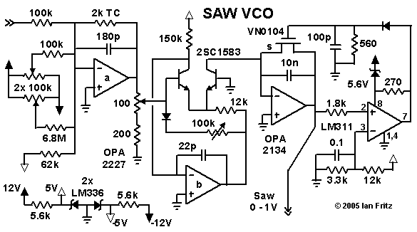
Let’s leave Buchlaland and look at a sawtooth core oscillators.
Most sawtooth core VCO used JFETs as the discharging capacitor. Ian Fritz
has been experimenting with using MOSFETs instead. Some of his latest
experiments are shown
here.
Notice Ian is using LM336s to set precise voltage references.
a) Is the MOSFET an n-channel or a p-channel MOSFET?
b) Assuming perfect “zero tolerance” resistors, compute
the threshold set at the negative terminal of the LM311 to
three places after the decimal point. Of course, with practical resistors,
this is “close enough to 1 V. (Don’t worry about the capacitor; it’s just
there to bypass assorted unwanted goo.)
c) Let’s call the current flowing into the collector of the right
transistor of the 2SC1583 NPN pair (that’s what’s used in the Roland
TB-303; they’re out of production, but
Limor
is
selling leftovers from her
xoxbox project;
I’ll get some for you to play with) “Icon,” where “con” is a subscript.
Find the value of Icon that would give a pitch of 4186 Hz, which is
corresponds to the highest note available (a “C”) on a standard piano.
d) When the sawtooth wave < 1 V, what voltage is applied to the MOSFET
gate?
e) When the sawtooth wave exceeds 1 V, what voltage is applied to the
MOSFET gate? Remember in this case, the LM311 “lets go” of its
“open collector” output. Assume the diode in the upper right hand corner
has a drop of 0.7 V, and ignore the 100 pF cap. Note that Ian is using
a 5.6 V zener to set a voltage of 6.4 V at pin 8 of the LM311.